|
<< Click to Display Table of Contents > Gate, LaserA, LaserB |
  
|
|
<< Click to Display Table of Contents > Gate, LaserA, LaserB |
|
All 3 outputs can operate in opto-insulated mode. For this the LASER_Opto_VCC (pin 11) and LASER_Opto_GND (pin 30) must provide the supply. LASER_Opto_VCC may not exceed +5 V with respect to LASER_Opto_GND.
As default the optocouplers take their supply from internal VCC, which causes to eliminate the opto insulation. In this case the voltage of all 3 outputs are TTL compatible in respect to GND. The mode can be selected by jumpers JP1 (GND), JP2 (VCC) as shown in figures 9 and 10.
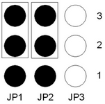
Figure 9: Laser signal optocoupler external supply
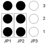
Figure 10: Laser signal optocoupler internal supply (default)
The polarity of the Gate, LaserA and LaserB outputs is selected with jumper JP3 as shown in figures 11 and 12.
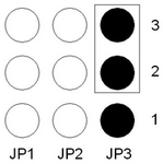
Figure 11: Laser signal polarity active low (default)
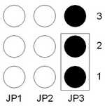
Figure 12: Laser signal polarity active high
|
During USC-1 startup and when the laser signals are disabled by software, the LaserGate, LaserA and LaserB will go into tri-state. It must be assured that the Laser defaults to a safe operation in this case. Potentially, a pull-up or pull-down resistor (about 4k7 ohm) has to be added to put the laser into a safe state. |
|---|
For YAG style laser mode the output timing (active low mode) is as follows:
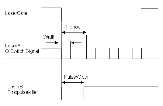
Figure 13: YAG laser control signals
The maximum output frequency for the LaserA and LaserB is 2 MHz, the period resolution is about 80 ns. The minimum output pulse width for LaserA and LaserB is about 167 ns.
